-
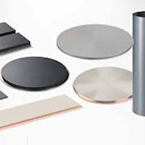
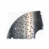
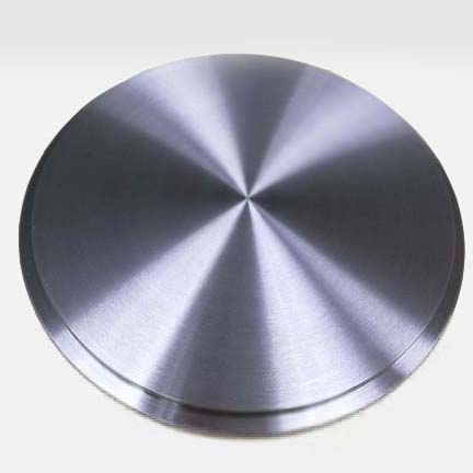
Sputtering Targets: Sputtering is an advanced thin-film material preparation technology. It utilizes ions generated from an ion source, accelerated and focused into a high-speed ion beam in a vacuum, which bombards the surface of a solid. The kinetic energy exchange between the ions and the atoms on the solid surface causes the atoms to leave the target and deposit onto the substrate, forming a nano (or micro) thin film. The solid being bombarded is the raw material for depositing thin films via sputtering, known as the sputtering target. Tungsten and molybdenum sputtering targets can form thin films on various substrates. These sputtered films are widely used in electronic components and products, such as TFT-LCDs (Thin Film Transistor-Liquid Crystal Displays), plasma display panels, inorganic light-emitting diode displays, field emission displays, thin-film solar cells, sensors, semiconductor devices, and field-effect transistor gates with tunable work function CMOS (Complementary Metal-Oxide-Semiconductor). The quality of a target is primarily determined by factors such as purity, density, grain size, and distribution. To ensure target quality: High-purity molybdenum powder is selected as the raw material. Rapid densification forming and sintering techniques are used to ensure low porosity and controlled grain size. Strict control over the introduction of impurity elements during the preparation process. For some high-demand products, hot isostatic pressing is employed, producing molybdenum-niobium targets with 95% to 99% high-density fine-grain products.
MOCVD: Metal-Organic Chemical Vapor Deposition (MOCVD) is a primary method for growing thin-layer single crystals of III-V and II-VI group compounds and alloys. Using hydrogen or nitrogen as carrier gases, vapors are carried out from liquids and mixed with group V hydrides (such as NH3, PH3, AsH3), then introduced into a reaction chamber where they react on a heated substrate surface to epitaxially grow compound crystal films. The core of LED light emission is a composite material known as an epitaxial slice. The successful application of MOCVD technology in epitaxial slices has led to a rapid increase in the use of such equipment. Since MOCVD equipment operates at temperatures above 2000°C, tungsten and molybdenum are also materials for some components of this equipment.
MOCVD: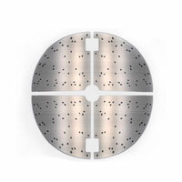
-
 Molybdenum and Tungsten materials possess high melting point, low vapor pressure, low coefficient of thermal expansion, along with excellent high-temperature strength and resistance to creep.
 -
 Ion implantation requires materials with high-temperature performance and resistance to chemical erosion. Tungsten molybdenum materials are predominantly used for the main components of ion chambers due to their excellent properties in these regards.
 -
 By adding a layer of molybdenum liner to the graphite crucible (molybdenum-lined crucible), the temperature of the crystal rod is controlled, thereby increasing the pulling speed of the crystal.
 -
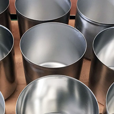 The main technical parameters of tungsten crucible spinning products are as follows: Density: 18.5±0.2 g/cm³. Composition: Compliant with national standards: ≥99.95%.
 -
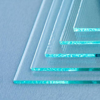
 The quartz glass melting and ceramic melting industries provide customers with mature and stable tungsten molybdenum components for high-temperature melting.
 -
We offer high-purity materials with exceptionally stable performance, ideal for growing various heterostructure materials and ultra-thin epitaxial layers.
-
 We provide tungsten molybdenum components for lighting technology manufacturing, primarily used in LED light source production, contributing to energy conservation and environmental protection.
 -
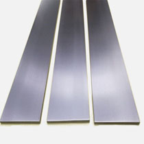
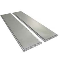
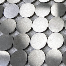
We offer high-purity sputtering targets with excellent density and corrosion resistance. Binding services are available.
-
 High-density tungsten-based alloys: W-Ni-Cu, W-Ni-Fe, Mo-Cu, W-Cu
 -
 In medical imaging, the molybdenum target receives X-rays and generates images. Molybdenum is also one of the key materials in X-ray tubes.
 -
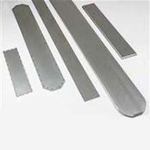
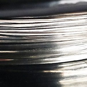 Tungsten ribbon, tungsten-molybdenum electrodes, tungsten-molybdenum alloy welding wire
 -
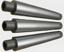
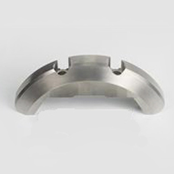
 Glass melting electrode; Molybdenum electrode arm; Tungsten-molybdenum material rack; Molybdenum heat shield; Tungsten-molybdenum crucible; Tungsten-molybdenum material table